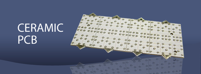

Thick Film technology is a widely used manufacturing process for ceramic circuit boards. Because of the advantageous properties of ceramic based substrates, thick film circuit boards are primarily used in harsh environmental conditions.
These include extreme high and low temperatures, thermal shock applications, high humidity, vibrations, acceleration, etc.
This technology also meets the requirements of high reliability and long lifetime.
Compared to traditional printed circuit boards, thick film ceramic substrates have better heat-conduction and have the
ability to match the coefficient of thermal expansion (CTE) with that of silicon chips. Because of these properties, it is
possible to create both High Density Packages (HDP) and miniaturized ones for various applications.
Areas of applications include Defense/Aerospace, Medical electronics, Micro-electronics, Automotive, etc.
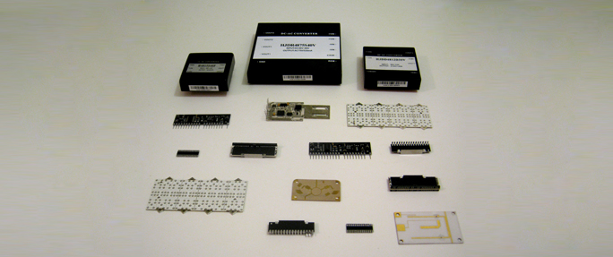
The products include:
• DC/DC converters and DC/AC power inverters
• Oscillator control modules
• Electronic control units (ECU) for automotive applications
• Solid State Relay (SSR) circuit boards
The standard thick film process usually involves screen printing, drying, and firing. The firing temperature is approximately
850°C, which guarantees the final film properties such as adhesive strength and electrical values.
At Complete Hermetics, multilayer substrates with several conductive layers on front and back of the substrates are available. Ceramic substrates may have variety of shapes and sizes up to 6” x 4.5”. Using a laser trimming process, thick film resistors
can be printed and adjusted from 0.1 to 150 M-Ohms. Resistors can be made within 0.1% tolerance thereby allowing for
precise voltages.
Substrate Materials:
• 96% & 99% Aluminum Oxide (Al2O3)
• Aluminum Nitride
• 96% BeO
Conductive Materials:
• Wire Bondable: Gold (4-7 M-Ohms)
• Solder Types: Palladium-Silver (20-30 M-Ohms)
• Solder Types: Gold and Platinum-Gold (50-60 M-Ohms)
• Minimum Track/Gap: 0.15mm
• Conductor Layers: 4 each side
• Printed via holes: Gold or Palladium-Silver
Resistors from 0.1 to 150 M-Ohms:
• Tolerance: +/- 0.1%
• Matched: +/- 0.1%
• Absolute TCR: +/- 100 ppm/°C standard
• Tracking: 10ppm/°C
• Power Dissipation: 0.05 w/mm2 at 125°C
• Voltage Handling: up to 40KV


